The MagLab is funded by the National Science Foundation and the State of Florida.
The MagLab is funded by the National Science Foundation and the State of Florida.
The Magnet Science & Technology division has facilities for components testing, mechanical & physical properties testing and microanlysis lab. Our materials scientists use the latest micro-characterization techniques to better understand and improve the micro/nano-structure of materials.
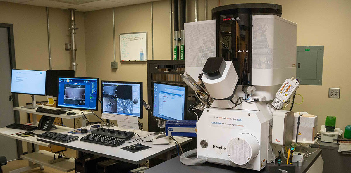
FIB-SEM Thermo Fisher Helios G4 UC microscope hosted by MagLab.
Watch an overview of the SEM and how it works.
The FEI Helios G4 UC is a multi-technique, dual beam (electron and Ga ion) Field Emission Scanning Electron Microscope (FESEM) with a spatial resolution for second electron imaging up to 0.6 nanometer. This interdisciplinary tool has many additional capabilities:
To book instruments or services, please check our calendar for the microscope schedule. You can see the schedules of instrument usage and available time slots.
View Calcium - Dual Beam Scanning Electron Microscope calendar
For more information on using this microscope, training and access, please contact Hannah Matos Pimentel.
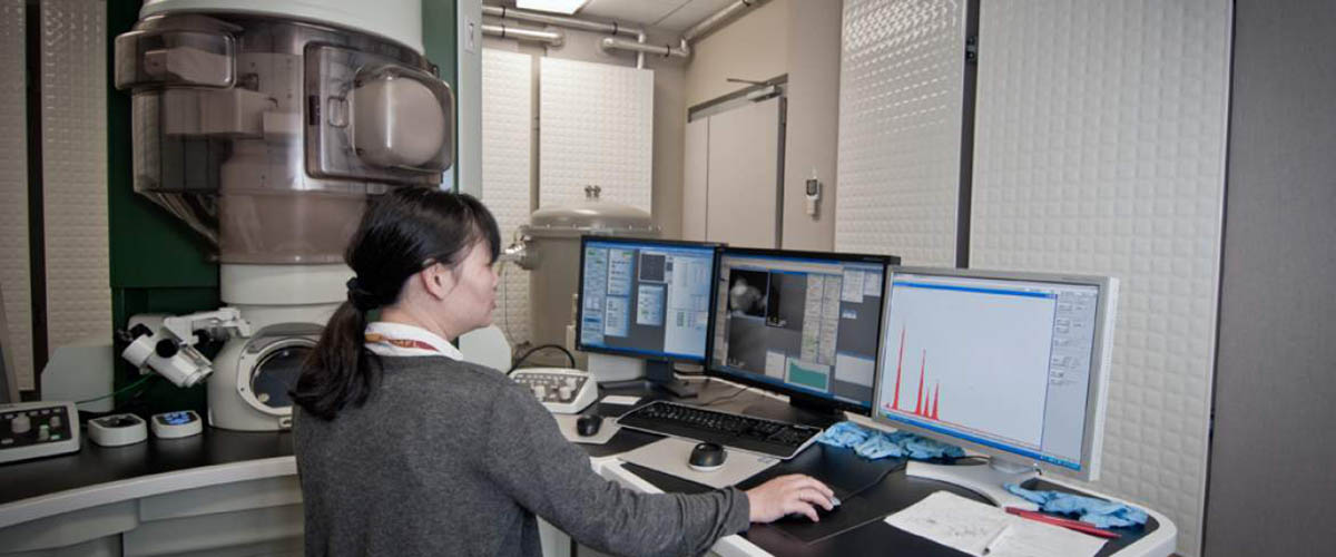
Scientist Yan Xin works on the JEM-ARM200cF
Watch an overview of the TEM and how it works.
This state-of-the-art s/TEM, incorporating a probe spherical aberration corrector for electron optic system and the maximum level of electrical and mechanical stability, has achieved a scanning transmission image (STEM-HAADF) resolution of 0.078 nm, the highest in the world among the commercial transmission electron microscopes.
The electron probe, after its aberrations are corrected, features a current density level higher by an order of magnitude than conventional transmission electron microscopes. With this probe finely focused, the ARM200F is capable of atomic level analysis. It operates at 200kV, 120kV and 80kV.
This microscope is equipped with the following:
For more information contact Yan Xin or visit the Transmission Electron Microscopy page on the Florida State University’s Office of Research website.
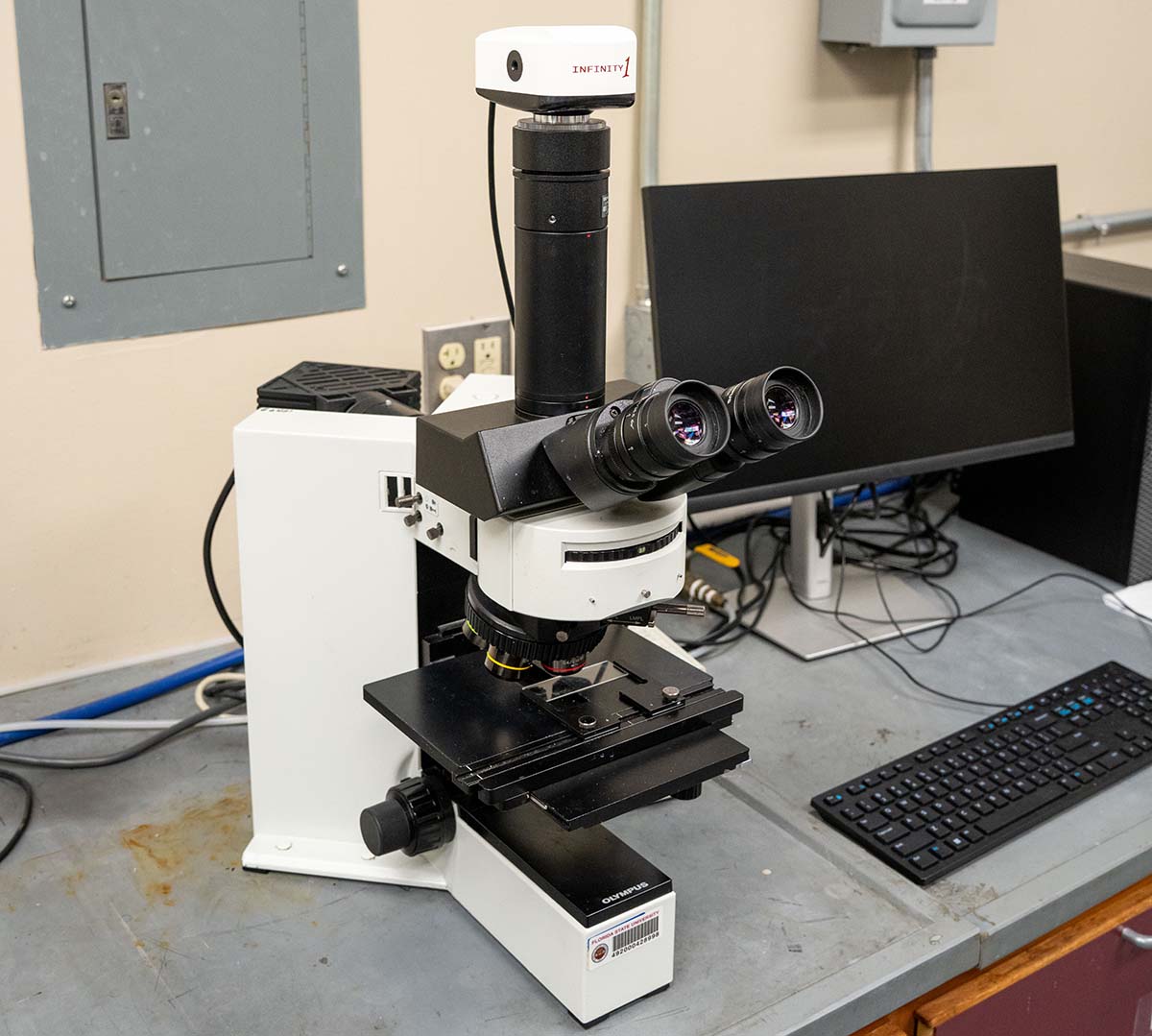
Olympus Optical Microscope
This optical microscope (Olympus BX60M) is equipped with reflected light and is powered by the 12v 100w lamphouse. The reflected light module features brightfield and darkfield settings and four reflected light Turret positions.
Additionally, the five-position nosepiece includes objective lenses with 5x, 10x, 20x, 50x, and 100x magnification levels.
For more information, please contact Hannah Matos Pimentel.
In recognition of the of the sample preparation importance in materials characterization, our laboratory has extensive facilities for metallographic, scanning electron microscopy (SEM), and transmission electron microscopy (TEM) sample preparation.
Components Testing Lab
Cell 16 is a laboratory specifically dedicated to testing magnet components and large conductors. It features superconducting magnets, high current and voltage power and direct access to the lab’s helium liquefier.
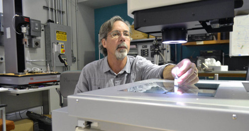
Research Associate Bob Walsh examines the fracture surface of a tensile specimen on an inspection microscope in the Mechanical and Physical Properties Lab.
Unique test equipment and methods are used by scientists to evaluate the performance of materials in extreme environments.
We also provide testing and analysis services to industry, universities and government agencies that require our experience and distinctive capabilities.
Equipment for testing mechanical properties includes:
Equipment for testing physical properties includes:
For more information on this capability please contact Jun Lu.
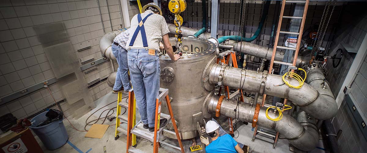
The cable-in-conduit conductor (CICC) magnet shop handles all of the MagLab’s CICC building and fabrication needs. The group undertakes a wide range of projects and tasks, from building coils that weigh 6 tons to welding tubes as small as 1/8-inch in diameter. The group’s main job is building large-scale superconducting magnets, a process that includes winding, heat treatment, vacuum-pressure impregnation (VPI) and final assembly.
During the winding process, engineers manipulate rectangular CICC that is cleaned and wrapped by machines, then wound into a cylinder to shape a coil. The coil is then placed into a furnace and reacted at 700 degrees Celsius. This month-long process transforms the coil into a superconducting magnet. Once reacted, the coil is placed in a vacuum chamber where the windings are filled with a special epoxy developed at the lab. This VPI process strengthens the coil, preparing it for the stresses it will undergo during operation. The final assembly includes tasks such as electric Paschen testing, induction welding and brazing, critical lifting, and helium leak testing. Many other detailed operations occur during the major processes, including milling and machining, tig and mig welding, cryogen testing and chemical etching.
In addition, the shop does jobs for other groups in the lab, including vacuum tight welding, helium leak tests, and general fabrication for magnet users.
For more information contact Todd Adkins.
This group builds all the resistive coils for new magnet installations as well as replacement coils for existing systems in the lab’s DC Field Facility. The group assembles an average 10 coils a year; in its first two decades, its total output has been some 240 coils.
The group’s recent projects include the lab’s 25 tesla split magnet — as of 2014 still the most complicated resistive magnet ever built — and the conical bore resistive insert for series connected hybrid magnet built for the Helmholz Centre Berlin. Featuring patented, world-leading conical bore technology, the insert was successfully tested to 13 tesla in June 2014. The shop is currently charged with the 4-coil resistive insert for the MagLab’s 36 tesla series connected hybrid, a system that will feature world-record field homogeneity thanks to the use of sophisticated axial current grading.
Responsibilities of the shop’s experienced staff include:
For more information contact Jack Toth.
In this space we build high-temperature superconductor (HTS) magnets. The room is set up with a programmable winder for both layer- wound and pancake-style windings. Joints, terminals etc. are also created here using specialized hardware, and all components are then assembled into complete systems that are ready for use. We focus on REBCO Coated Conductors to build coils for high-field magnets operating a low temperatures, starting with the 32 T all-superconducting magnet.
For more information contact Lee Marks.
The main machine shop covers 5,000 square feet and has a wide array of manufacturing equipment. Along with standard tool room machinery, the shop includes several 4-axis CNC mills, a CNC lathe, and a 6-axis wire EDM machine. Programming of the CNC machinery is aided by direct access to the MS&T design database. Manufactured parts vary in size from less than 1mm to the 1600mm X 800mm(X,Y) travel of the large NC mill. The six machinists have specialized skills in prototyping, fabricating scientific instrumentation and mechanical design.
For more information contact Edward Rubes.
The Engineering Analysis group consists of a team of physicists and engineers who support magnet and system design through high level analyses. Design problems are often solved through numerical techniques which includes a variety of software that have been developed both in-house and commercially. Some of the in-house codes have been specifically written to address the concerns of high-field superconducting and resistive coils and include:
The finite element method is often employed using ANSYS for coupled electromagnetic-thermal-structural models or Vector Fields for 3-D non-linear electromagnetic analyses. Thermo-hydraulic analysis of coils with cable-in-conduit conductors are performed using the customizable GANDALF software. If applicable, stringent design criteria are applied in the design of structures. These may include the ASME Boiler & Pressure Vessel Code, ASME Plumbing B31, ASME Below the Hook Lifting Devices, or fusion magnet structural design criteria.
For more information contact Iain Dixon.
The lab’s Engineering Design team tackles a wide variety of design applications and challenges. The team designs thousands of parts for the lab’s large magnet systems, such as the 45 tesla hybrid and the 900 MHz ultra wide bore magnets, as well as for systems under development. Each magnet project has unique requirements, and parts — some weighing a few grams, some more than a ton — must be designed to withstand considerable forces over the course of many years. The group is responsible for parts for resistive, superconducting and hybrid magnet systems, ranging from a simple test apparatus to complex hybrid superconducting systems.
Team engineers bring decades of experience to the job and skills that include CAD, Autodesk Inventor/Vault and ANSYS Workbench as well as analysis software.
For more information contact Todd Adkins.
The Magnet Science & Technology group typically manages several highly complicated magnet-building projects concurrently, and the group’s expertise in complex project management meets these demands. Using a methodology dubbed Project Management Improvement Program (PMIP), group administrators manage critical project parameters including cost, personnel resourcing and milestone schedules. The group’s scientists and engineers are continuously designing and building things that have never been done before — a challenge when predicting costs and schedules. Our structured approach to project management improves our ability to assess and manage risk and, in turn, to meet cost and schedule goals while continuing to break world records.
Last modified on 07 April 2026