What is the finding?
Studing the micro- and nano- structure properties in multiple round wires made with Bi-2212, researchers learned that processing controls impact grain orientation and grain boundary composition in Bi-2212 Round Wire to improve superconducting critical current density (Jc).
Why is this important?
High-magnetic-field applications of Bi-2212 Round Wire will require a knowledge of how nanostructure influences the critical current density (Jc) and how this nanostructure can be optimized during the heat treatment processing of Bi-2212 Round Wire. The goal is to push Bi-2212 to the forefront of high temperature superconductors (HTS) to make next generation superconducting magnets that can be operated at higher fields, higher temperatures, and at lower cost.
Who did the research?
T.A. Oloye1,2, M. Matras4, J. Jiang1, S.I. Hossain1,2, Y. Su1,*, U. P. Trociewitz1, E. E. Hellstrom1,2,3, D. C. Larbalestier1,2,3, and F. Kametani1,2,3
1Applied Superconductivity Center, MagLab; 2Materials Science and Engineering, FSU; 3FAMU-FSU Dept of Mechanical Engineering; 4European Organization for Nuclear Research; * Now: Materials Science and Technology Division, Oak Ridge Nat'l Lab
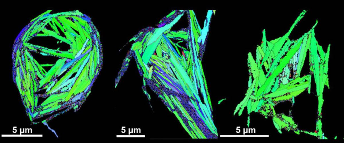
Why did this research need the MagLab?
The MagLab's Applied Superconductivity Center provided both the expertise and the nanoscale imaging tools - Electron Back Scatter Diffraction (EBSD) and Transmission Electron Microscopy (TEM) – necessary to link critical current densities to nanostructure. The EBSD enabled us to visualize the important high Jc grain microstructures within the individual filaments, while the TEM revealed the nanostructural features of grain boundaries that are also necessary to develop high Jc.
Details for scientists
- View or download the expert-level Science Highlight, Advanced Microscopy for Better Nanostructural Insights in Bi-2212 Round Wires
- Read the full-length publication, Correlation of critical current density to quasi-biaxial texture and grain boundary cleanliness in fully dense Bi-2212 wires, in Superconductor Science and Technology
Funding
This research was funded by the following grants: D. C. Larbalestier, E.E. Hellstrom, J. Jiang and F. Kametani (DOE DE-SC0010421) and G.S. Boebinger (NSF DMR-1644779)
For more information, contact Lance Cooley.