
Schematic and Powerpoint
| Thumbnail View | Image Link | Description |
|---|---|---|
 |
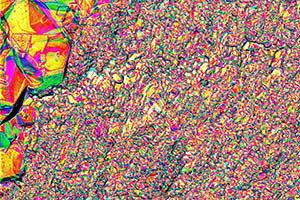
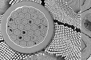
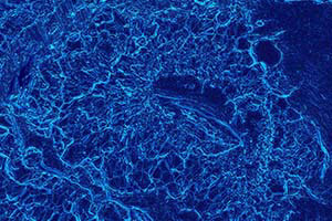
Animated Powerpoint slide showing a deep metallographic zoom into an ITER CS conductor after testing in the high field zone of the SULTAN testing facility. Images by Charlie Sanabria. SULTAN-tested cable was provided by courtesy of Pierluigi Bruzzone (Plasma Physics Research Center) with agreement from Fusion for Energy. The CSJA2 cable was also provided by arrangement with the Japan Atomic Energy Agency (JAEA), Superconductor Technology Group, Division of Fusion Energy Technology. This is a considerably extended version of a slide originally presented as part of talk 3OrBB-07 by Peter J. Lee at MT-23, Wednesday, July 17, 2013. | |
 |
pptx - 876KB | Animated Powerpoint slide showing the components of an ITER TF conductor. Images by Charlie Sanabria. SULTAN-tested cable was provided by courtesy of Pierluigi Bruzzone (Plasma Physics Research Center). Originally presented as part of talk "Understanding the Performance Degradation of CICC Conductors for ITER Under Testing in the SULTAN Facility" presented April 19th 2013 at NHMFL and 3OrBB-07 at MT-23, Wednesday, July 17, 2013 by Peter J. Lee. |
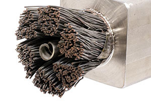 |
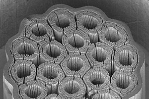
JPG - 1.3MB | ITER CS conductor after partial removal of the stainless steel jcket to reveal in the internal components. Images by Charlie Sanabria. SULTAN-tested cable was provided by courtesy of Pierluigi Bruzzone (Plasma Physics Research Center) with agreement from Fusion for Energy.
|
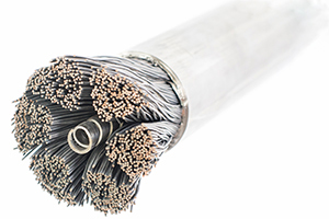 |
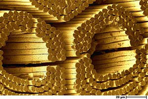
JPG - 1.7MB | ITER TF conductor after partial removal of the stainless steel jcket to reveal in the internal components. Images by Charlie Sanabria. SULTAN-tested cable was provided by courtesy of Pierluigi Bruzzone (Plasma Physics Research Center) with agreement from Fusion for Energy.
|
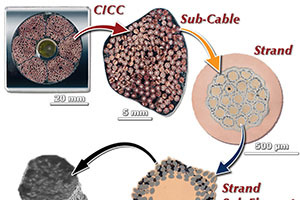 |
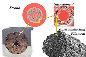
1024x909 382KB - JPG | 2008 CICC Montage showing the components of a Superconducting Cable-In-Conduit Conductor for ITER. Also available as: 2.4 MB Powerpoint 374 kB Transparent GIF (1024w x 909h) 1.4 MB Transparent PNG (1024w x 909h) Higher resolution versions are available. |
 |
1198x898 324KB - JPG | Older montage showing the components of a Superconducting Cable-In-Conduit for ITER Model Coil Program (1996). IGC-AS (now Luvata) strand shown. This older version still shows up in presentations and publications and is kept here for archival puroposes. |
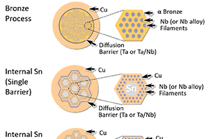 |
1238x1414 100KB -PNG | Schematic diagram illustrating the four major designs of commercial Nb3Sn strand. Higher resolution versions available. |
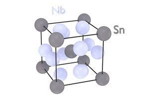 |
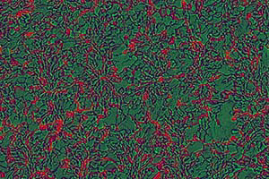
616x584 171KB -PNG | Nb3Sn forms a crystalline intermetallic compound with an A15 structure consisting of a BCC sub-lattice of Sn atoms and a pair of Nb atoms on each face.
|

2D Images
| Thumbnail View | Image Link | Description |
|---|---|---|
 |
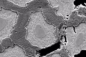
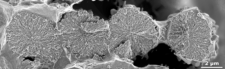
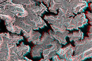
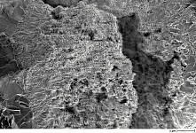
588x831 132KB - JPG | A fracture cross-section of a partially reacted Nb3Sn filament (TWC MJR strand). MJR (modified jelly-roll) is a type of internal-Sn strand that is no longer manufactured. |
 |
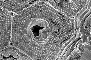
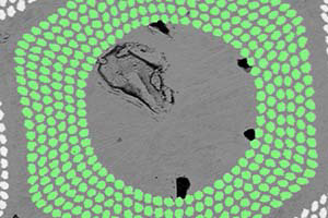
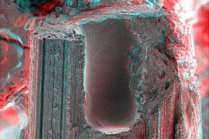
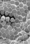
424x608 128KB - JPG | Golden Ears of Nb3Sn Corn II (IGC-AS Internal Sn ITER strand). Occasionally the fracture-cross-section process pulls out a filament and exposes the surface facets of the outermost Nb3Sn grains.† [False-color] |
 |
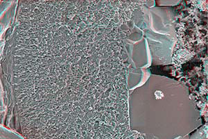
False color fractograph of SMI PIT Nb3Sn A15 layer. FESEM image colored for effect (a rejected image for the annual ASC Holiday/New Year card). Unreacted strand supplied to the UW by Shapemetal Innovation B. V., Enschede, The Netherlands. | |
 |
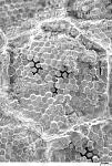
False color image of filaments in polished cross-section of Furukawa ITER Nb3Sn strand. Note the exceptional uniformity and the barely discernable extra spacing between the original bundles of 19 filaments. | |
 |
Another false color variant on the Furukawa ITER strand. The unreacted Nb cores (green) are more visible here. FESEM image. | |
 |
False color images of Nb3Sn filament extracted for IGC-AS ITER strand. FESEM image. The filament as approximately 1/25 the thickness of a sheet of paper. | |
 |
Montage showing design of IGC-AS high Jc (critical current density) internal Sn strand. Heat treated strand supplied to the UW by IGC-Advanced Superconductors, Waterbury, CT. | |
 |
Deep etch of IGC-AS internal Sn strand (Cu removed by etch). | |
 |
False color FESEM image of deep-etch IGC-AS Nb3Sn strand. | |
 |
A windows background image showing Nb3Sn filaments exposed by deep Cu etch. | |
 |
False color image showing filaments in unreacted MJR sub-element: TWC MJR Nb3Sn. | |
 |
Etch cross-section of LMI Nb3Sn strand for ITER showing partially reacted filaments with columnar interior A15 grains. FESEM. | |
 |
False color image of fully reacted filament from LMI-ITER Nb3Sn strand. | |
 |
LMI strand for ITER. Etched partial cross-section showing three filaments adjacent to the diffusion barrier. FESEM. | |
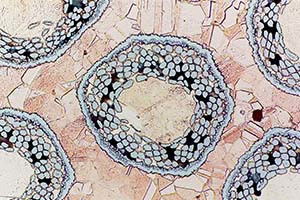 |
Light microscope image of LMI Nb3Sn prototype strand for ITER showing sub-elements of Nb3Sn filaments surrounded by diffusion barriers. | |
 |
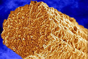
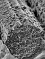
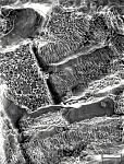
A really big FESEM fractograph of a Mitsubishi prototype Nb3Sn strand for ITER. The filaments from this composite were particularly uniform and the properties were the best of the ITER developmental program. | |
 |
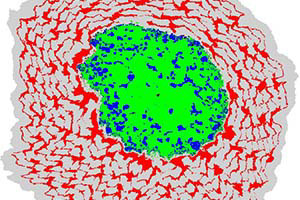
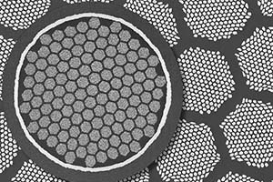
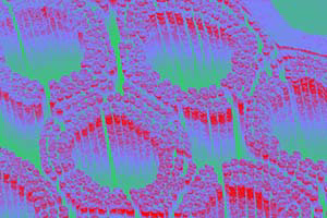
A polished transverse cross-section of a Mitsubishi ITER Nb3Sn strand has been imaged by FESEM and then analyzed for filament size, uniformity and distribution (which in this case is particularly good). The analyzed filaments are highlighted in green. | |
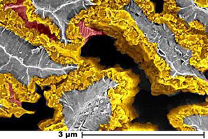 |
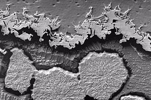
False color fractograph of OI-ST high critical current density MJR Nb3Sn A15 layer. The strand has been ramped to final heat treatment temperature but has received its final HT. The Cu (red) and A15 (gold) colors have been added to help distinguish the components. FESEM. Unreacted strand supplied to the UW by Oxford Instruments Inc. - Superconducting Technology, Carteret, NJ. | |
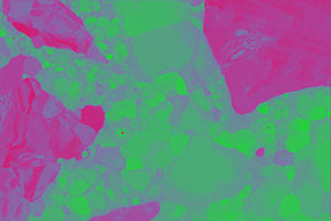 |
False color electron backscatter image of bulk Nb3Sn produced by HIP'ing powders at the UW-Madison. This is a two phase region with unreacted Nb in purple and Nb3Sn in green. FESEM. | |
 |
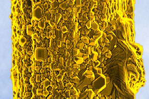
False color image of VAC bronze process Nb3Sn filament after partial reaction. This highly distorted filament is unrepresentative of the otherwise excellent composite but of course it looks more interesting. FESEM. Strand courtesy of Vacuumschmelze GMBH, Hanau, Germany. | |
 |
Transverse cross-section of VAC bronze-process Nb3Sn strand superimposed on detail showing filaments of Nb3Sn in sub-element groupings. FESEM. Strand courtesy of Vacuumschmelze GMBH, Hanau, Germany | |
 |
False color image of Nb3Sn filaments in a IGC-AS strand exposed by a deep Cu etch. | |
 |
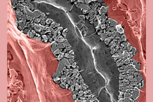
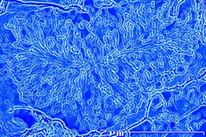
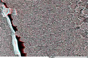
1536x460 428KB - 2 - JPG | Superconductor Rope Trick. For high magnetic field use, multifilamentary strands must be twisted so that eddy current losses, and flux jump and self-field instabilities are minimized. This produces the twisted rope appearance when viewed in longitudinal cross-section (FESEM-Electron Backscatter Image) of this Nb3Sn strand manufactured by IGC-AS (now Outokumpu Advanced Superconductors). |
 |
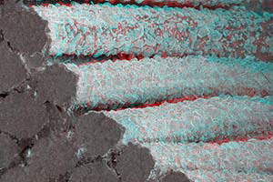
1024x1280 689KB - JPG | Strand used to produce record high field (16.1 T, 4.2 K). accelerator dipole magnet at LBNL. The strand has been fractured and imaged using an in-lens secondary electron detector in a FESEM in order to reveal grain size. The red and green channels have been processed by "Difference of Gaussians" and "Local Equalization" under Fovea Pro in order to enhance grain boundary contrast. The petal-like pattern originates from the original Nb filaments that were fused together during the reaction to for Nb3Sn. Strand manufactured by OI-ST and heat treated by Dan Dietderich and Ron Scanlan at LBNL. |
3D Images
These image are vieweable in 3D using traditional red-blue glasses (typical of glasses used for 1950s horror movies).
The yellow/blue glasses provide better 3D viewing of color images and are provided free at the Applied Superconductivity Center during the annual Open House. You may also have these cardboard glasses from advertising promotions.
| Thumbnail View | Image Link | Description |
|---|---|---|
 |
480x613 289KB - JPG | A fracture cross-section of a partially reacted Nb3Sn filament (TWC MJR strand). MJR (modified jelly-roll) is a type of internal-Sn strand that is no longer manufactured. |
 |
Golden Ears of Nb3Sn Corn II (IGC-AS Internal Sn ITER strand). Occasionally the fracture-cross-section process pulls out a filament and exposes the surface facets of the outermost Nb3Sn grains.† [False-color] | |
 |
False color fractograph of SMI PIT Nb3Sn A15 layer. FESEM image colored for effect (a rejected image for the annual ASC Holiday/New Year card). Unreacted strand supplied to the UW by Shapemetal Innovation B. V., Enschede, The Netherlands. | |
 |
False color image of filaments in polished cross-section of Furukawa ITER Nb3Sn strand. Note the exceptional uniformity and the barely discernable extra spacing between the original bundles of 19 filaments. | |
 |
Another false color variant on the Furukawa ITER strand. The unreacted Nb cores (green) are more visible here. FESEM image. | |
 |
False color images of Nb3Sn filament extracted for IGC-AS ITER strand. FESEM image. The filament as approximately 1/25 the thickness of a sheet of paper. | |
 |
Montage showing design of IGC-AS high Jc (critical current density) internal Sn strand. Heat treated strand supplied to the UW by IGC-Advanced Superconductors, Waterbury, CT. | |
 |
Deep etch of IGC-AS internal Sn strand (Cu removed by etch). | |
 |
False color FESEM image of deep-etch IGC-AS Nb3Sn strand. | |
 |
A windows background image showing Nb3Sn filaments exposed by deep Cu etch. | |
 |
False color image showing filaments in unreacted MJR sub-element: TWC MJR Nb3Sn. | |
 |
Etch cross-section of LMI Nb3Sn strand for ITER showing partially reacted filaments with columnar interior A15 grains. FESEM. | |
 |
False color image of fully reacted filament from LMI-ITER Nb3Sn strand. | |
 |
LMI strand for ITER. Etched partial cross-section showing three filaments adjacent to the diffusion barrier. FESEM. | |
 |
Light microscope image of LMI Nb3Sn prototype strand for ITER showing sub-elements of Nb3Sn filaments surrounded by diffusion barriers. | |
 |
A really big FESEM fractograph of a Mitsubishi prototype Nb3Sn strand for ITER. The filaments from this composite were particularly uniform and the properties were the best of the ITER developmental program. | |
 |
A polished transverse cross-section of a Mitsubishi ITER Nb3Sn strand has been imaged by FESEM and then analyzed for filament size, uniformity and distribution (which in this case is particularly good). The analyzed filaments are highlighted in green. | |
 |
False color fractograph of OI-ST high critical current density MJR Nb3Sn A15 layer. The strand has been ramped to final heat treatment temperature but has received its final HT. The Cu (red) and A15 (gold) colors have been added to help distinguish the components. FESEM. Unreacted strand supplied to the UW by Oxford Instruments Inc. - Superconducting Technology, Carteret, NJ. | |
 |
False color electron backscatter image of bulk Nb3Sn produced by HIP'ing powders at the UW-Madison. This is a two phase region with unreacted Nb in purple and Nb3Sn in green. FESEM. | |
 |
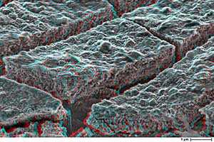
620x675 180KB - JPG | False color image of VAC bronze process Nb3Sn filament after partial reaction. This highly distorted filament is unrepresentative of the otherwise excellent composite but of course it looks more interesting. FESEM. Strand courtesy of Vacuumschmelze GMBH, Hanau, Germany. |
 |
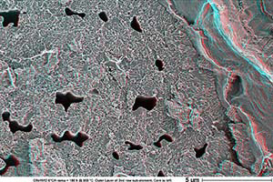
765x760 153KB - JPG | Transverse cross-section of VAC bronze-process Nb3Sn strand superimposed on detail showing filaments of Nb3Sn in sub-element groupings. FESEM. Strand courtesy of Vacuumschmelze GMBH, Hanau, Germany |