
Handbook of Superconducting Materials
A detailed explanation of these images will appear in “An Introduction to Digital Image Analysis of Superconductors” by C. Sanabria and P. J. Lee to be published in the Handbook of Superconducting Materials, Second Edition (Taylor and Francis, 2016, co-chief-edited by D. A. Cardwell and D. C. Larbalestier).

This work by The Applied Superconductivity Center is licensed under a Creative Commons Attribution 4.0 International License.
Based on a work at https://nationalmaglab.org/.
| Thumbnail View | Image Link | Description |
|---|---|---|
 |
1417x1039 661KB - PNG |
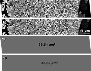
Different sample preparation techniquesLight microscope images of the same region of an unreacted Internal Tin Nb3Sn strand showing Nb rods inside a Cu matrix after the application of good (a) and bad (b) polishing procedures. (c) and (d) show the apparent isolated rod cross sections from (a) and (b) respectively; the dimensional difference quantified in d) is an artificial effect obtained from a poor metallographic preparation. The sample in (b) was polished using excessive force. |
 |
1417x1062 1.1MB - JPG |
Minor scratchesAn image of sub elements in a fully reacted RRP® Nb3Sn strand with a minor scratch produced during the final polishing stages or sample cleaning. |
 |
1414x1085 1.6MB - PNG |
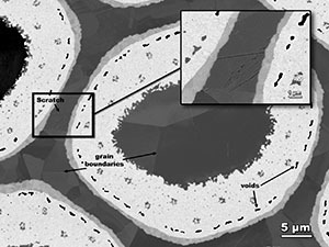
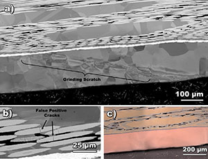
Buried damage(a) A longitudinal cross section of a Nb3Sn ITER strand after cyclic testing in the SULTAN facility is imaged using a backscattered electron detector in an FESEM. Cold work introduced by a hard particle during polishing is evident from the strain contrast. These samples are used to assess the damage caused by cyclic strains. Without the evidence of the scratch, false positive filament fractures shown in (b) could be misinterpreted as being due to the testing. The light micrograph in (c) shows the same region where the buried scratch is not detected. |
 |
1417x774 629KB - PNG |
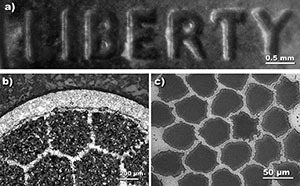
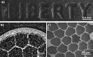
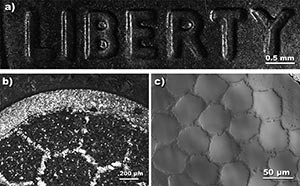
Different sample preparation techniques (2)Images of the same Bi 2212 strand (fabricated by Oxford Superconducting Technologies, OST) showing significantly different contents of voids (or bubbles) depending on the polishing technique. The image in (a) is a properly prepared sample and the image in (b) is a sample prepared using excessive force and short polishing times. |
 |
1417x878-1 1.1MB - PNG | |
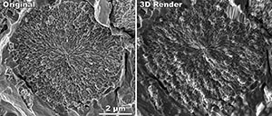 |
1417x604 600KB - PNG |
3D renderingA fractograph (in lens secondary electron image) of a filament from a Nb3Sn strand (left) compared with a 3D rendering of the filament showing the non planar nature of the fracture. |
 |
1417x878-1 1.2MB - PNG |
|
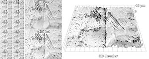 |
1417x560 372KB - PNG |
Three dimensional stackingIn this focus stack example 14 images of a grain boundary in a chemically polished Nb sample have been combined to produce both a fully focused output image and 3D rendering of the surface. |
 |
1417x878 1.3MB - PNG |
|
 |
1417x878-2 1.1MB - PNG |
Shallow depth of fieldImages with poorly focused areas due to (a) the slanted orientation of a penny, (b) etched off silver on a Bi 2212 strand (produced by OST) and (c) the slanted sample of Nb rods inside a Cu matrix (precursors of RRP® strands). |
 |
1417x878-2 1.2MB - PNG |
|
 |
1417x878-1 1.0MB - PNG |
Focus stack algorithmImages of the same area as those in "Shallow depth of field" corrected for focusing using an open source ‘focus stack’ algorithm. |
 |
1417x1113 1.8MB - PNG |
|
 |
1417x878-2 1.0MB - PNG |
OLYMPUS Stream Motion®Images of the same area as those in "Shallow depth of field" corrected for focusing using OLYMPUS Stream Motion®. |
 |
1042x587 450KB - PNG |
|
 |
1417x878-3 1.0MB - PNG |
Olympus Laser Scanning Confocal MicroscopeImages of the same area as those in "Shallow depth of field" corrected for focusing using an Olympus Laser Scanning Confocal Microscope. |
 |
1417x531 629KB - PNG |
|
 |
1417x570 144KB - PNG |
SEM drift(a) A backscatter electron image of an artificial pinning center in a Nb-Ti strand at an intermediate stage in wire drawing. This image is compressed during acquisition and distorted by upwards and lateral movement. (b) A drift corrected version of the same image using a fast scan image underlay (for reference) shows that the pin is less aspected than suggested by the original image. |
 |
1417x1230 1.5MB - PNG |
|
 |
1042x587 433KB - PNG |
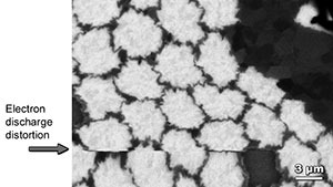
SEM chargingAn image of Nb filaments inside a Cu matrix (precursors of RRP® strands) showing a sudden electron discharge affecting the image scan. |
 |
1417x523 152KB - PNG |
|
 |
1417x531 657KB - PNG |
SE2 vs BSDTransverse cross sectional images of an Internal Tin Nb3Sn strand designed for ITER. (a) SE image and (b) BSE image. |
 |
1417x519 406KB - PNG |
|
 |
1417x1230 921KB - PNG |
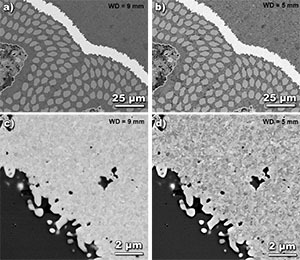
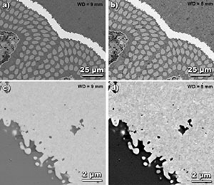
Working distance(a) and (b): backscattered electron images of the filamentary area of a Nb3Sn ITER strand before reaction taken at a working distance of (a) 9 mm with good phase contrast and another one with a working distance of (b) 5 mm showing higher grain contrast. Similar cases in (c) and (d) of a Nb3Sn layer of an RRP® strand. |
 |
1417x840 244KB - PNG |
|
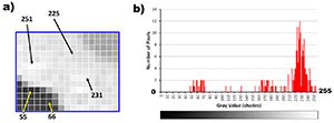 |
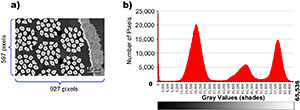
1417x523 96KB - PNG |
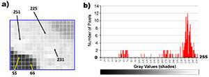
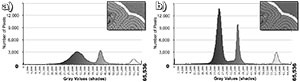
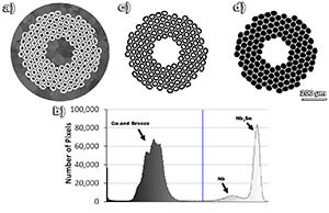
Simple histogram(a) A 221 pixel image showing some gray values and (b) the histogram of the image in 8 bit space (256 levels of gray). |
 |
1417x389 197KB - PNG |
|
 |
1417x519 282KB - PNG |
Complex histogram(a) a backscattered electron image of the filamentary area of Nb3Sn ITER strand taken in 16 bit space showing (b) the histogram of the image. |
 |
1417x389 170KB - PNG |
|
 |
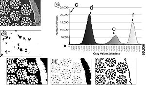
1417x840 147KB - PNG |
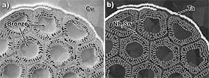
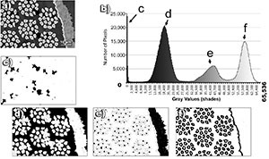
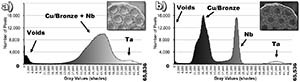
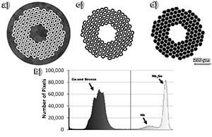
Feature recognition(a) SEM image of a Nb3Sn ITER strand and its (b) histogram showing different regions of gray values which can be easily separated into black objects representing (c) voids (d) bronze and Cu (e) Niobium and (f) Nb3Sn. |
 |
1417x1351 285KB - PNG |
|
 |
1417x389 124KB - PNG |
SE2 vs BSD (2)Histograms of (a) an SE image and (b) a BSE image of the same Nb3Sn strand cross sectional area. |
 |
1417x914 495KB - PNG |
|
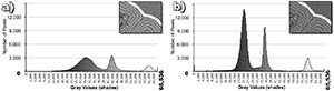 |
1417x389 102KB - PNG |
Working distance (2)Fiji's default threshold applied to an image as is as well as to different selections that are more convenient and accurate as shown by the histogram and the resulting binary images. |
 |
1417x350 267KB - PNG |
|
 |
1417x1351 300KB - PNG |
ThresholdingFiji's default threshold applied to an image as is as well as to different selections that are more convenient and accurate as shown by the histogram and the resulting binary images. |
 |
1417x452 183KB - PNG |
|
 |
1417x914 244KB - PNG |
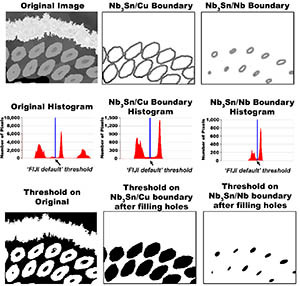
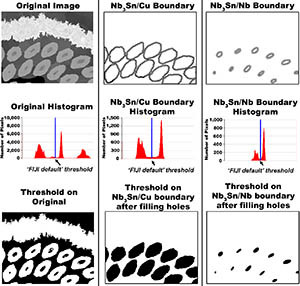
Fill holes(a) a transverse cross section of a fully reacted RRP® strand to which an automated threshold on the full image has been applied, producing an acceptable guess between the two main regions of the (b) histogram. This threshold resulted in a (c) binary image to which a fill holes algorithm can be applied to produce a (d) binary image of the subelement features in their entirety. |
 |
1417x1044 349KB - PNG |
|
 |
1417x415 534KB - PNG |
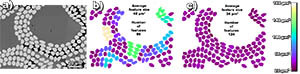
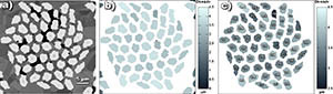
Watershed segmentation(a) Nb3Sn filaments of an ITER strand slightly bonded during reaction. The filaments were isolated into binary images (not shown) which were then measured and (b) shaded by area for the filaments as thresholded (left) and as separated by watershed segmentation (right). In (c) the shading was reapplied across the corrected range, showing a much more valuable piece of information, that the filaments closer to the center show the widest variation in area. Notice that the color scales of (b) and (c) are different. |
 |
1417x862 267KB - PNG |
|
 |
1417x401 1.3MB - PNG |
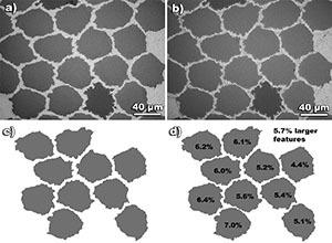
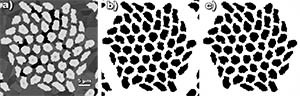
Reject features(a) Nb3Sn filaments of an ITER strand. The filaments were isolated into binary images where which were the filament features are shown (b) as thresholded and (c) rejecting features smaller than 100 pixels and those one the image edges. The objects are color coded according to their area equivalent diameters. Once again, the corrected range shows more valuable information as the variation is more easily seen. Notice that the color scales of (b) and (c) are different. |
 |
1920x1080 322KB - PNG |
|
 |
1417x1044 333KB - PNG |
Outlines(a) the Ta barrier of an ITER strand. The barrier isolated into a (b) binary image to which an outline algorithm was applied producing (c) pixel thick lines in the innermost boundaries of the barrier. |
 |
1417x997 128KB - PNG |
|
 |
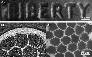
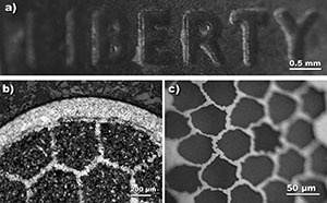
1417x862 98KB - PNG |
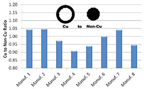
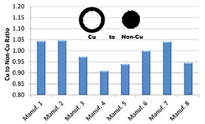
Area fractionsCu to Non‑Cu ratios of all eight ITER strand manufacturers |
 |
1421x998 255KB - PNG |
|
 |
1417x797 229KB - PNG |
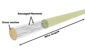
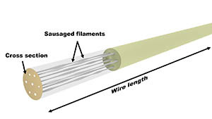
SausagingSketch of a wire length depicting very dramatic filament sausaging. |
 |
1417x1357 113KB - PNG |
|
 |
1417x997 113KB - PNG |
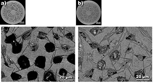
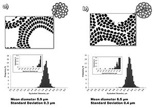
Equivalent diameterBinary images of Nb3Sn filaments of two ITER manufacturers (more than 1000 filaments each). The wire on the right shows has locally pinched filaments that contribute to larger standard deviation. |
 |
1417x998 222KB - PNG |
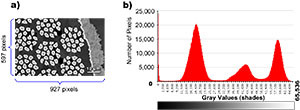
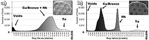
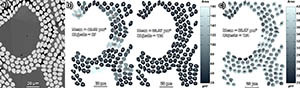
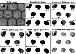
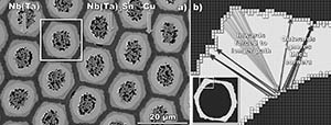
Area fractions (2)(a) An SEM image of RRP® sub elements during reaction having three different phases inside the cores (namely the Cu Sn phases η and ε, as well as voids). (b) A binary image of the cores used to establish the regions of interest and to measure the areas of each. The different phases are shown in (c), (d) and (e) colored using a gray value of 100 and leaving the rest black, these images are used to calculate the percentage of each phase in the cores. (e) A composite image of all phases colored for emphasis. |
 |
1417x784 473KB - PNG |
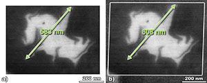
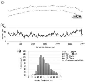
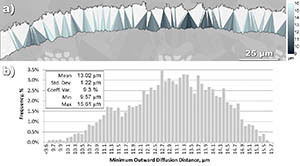
Shortest distance measurement(a) A Ta diffusion barrier in a Nb3Sn ITER strand has been outline and the minimum outward diffusion distances have been obtained using a macro (the minimum distance lines have been color coded according to length). In (b) we show the statistical distribution of the measured distances. |
 |
1417x539 427KB - PNG |
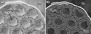
Inwards vs outwards(a) FESEM BSE detail from a cross section of a Powder in tube (SMI) Nb3Sn strand. (b) Illustration of how the direction of point to point thickness measurement varies with the location of the origin points for the measurements. |
 |
1417x451 637KB - PNG |
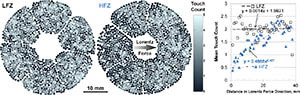
Touch countIn this analysis of strands in a prototype ITER TF cable after testing in the SULTAN facility we contrast cross sections from the low and high field zones (LFZ and HFZ respectively) using a count how many filaments are in contact with each other to estimate the local mechanical support and freedom to move. The repeated Lorentz force cycling separates the filaments out in the HFZ in the direction opposite to the Lorentz force. |
 |
1417x720 526 KB - PNG |
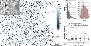
Size distributionsThis FESEM BSE image a) of the edge of a prototype Nb 44Ti 17Ta filament after final heat treatment shows the change in α Ti precipitate size with proximity to the edge. In b) the precipitates have been color coded according to their d* (diameter calculated from area). In c) and d) we contrast their size distribution in normal space and log space and clearly the distribution is closer to log normal. In e) we show the trend in mean d* with distance from the Cu/filament interface, contrasting the difference between linear and log results. This strand was manufactured by IGC AS as part of the FNAL LHC High Gradient Quadrupole Conductor program. |