What did scientists discover?
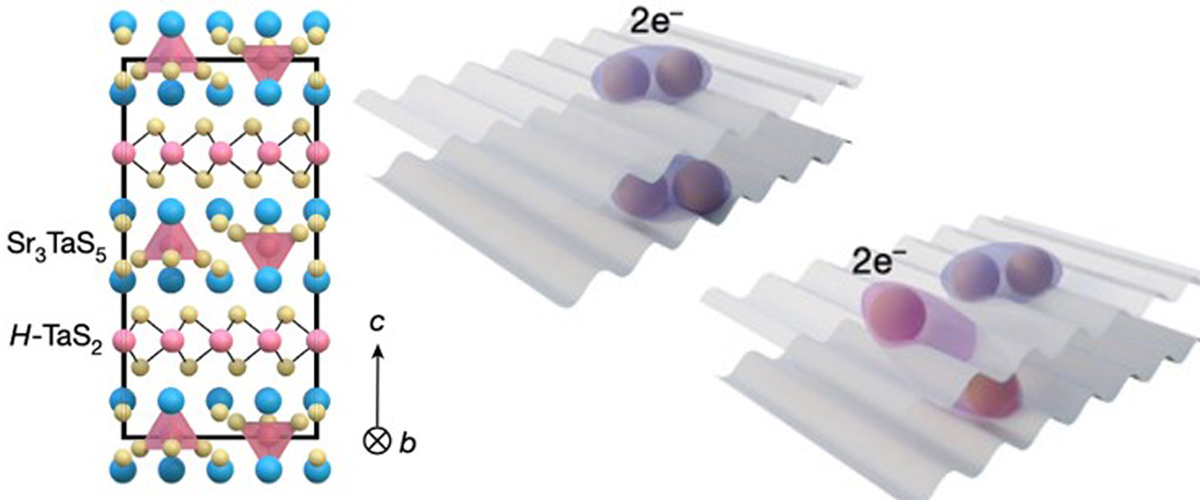
Scientists measured the Fermi surface of bulk crystalline SrTa2S5 to understand unique superconducting behaviors inside and between the material’s layers. Measurements showed that a unique mismatch between its layers affects the material's electronic states. This leads to surprising behaviors in electron mobility, quantum oscillations, and superconductivity.
Why is this important?
The properties of everyday materials (like metals, glass, and plastics) depend on how their electrons interact, either as free-moving valence electrons or bound in orbits around atoms. Understanding these interactions is crucial for developing new technologies and improving existing ones.
Who did the research?
A. Devarakonda 1,6, A. Chen1, D. Graf2, M. Kriener3, A.J. Akey4, D.C. Bell4, T. Suzuki5, J.G. Checkelsky1
1MIT; 2National MagLab; 3RIKEN; 4Harvard University; 5Toho University; 6Columbia University
Why did they need the MagLab?
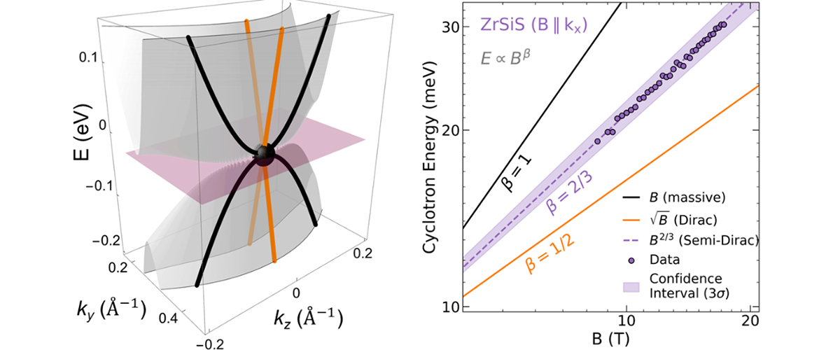
The Fermi surface is a mathematical model that shows the energy level dividing occupied (bound) electron states from empty (unbound) ones, determining many properties of conducting materials. To measure the Fermi surface's size and shape, one of the best methods is to place the material in a changing magnetic field and measure the resulting quantum oscillations in magnetization, susceptibility, or resistance. Using a 31T magnet and a low-temperature cryostat, researchers gathered data to map the Fermi surface of SrTa2S5 and compare it to calculations. Achieving this requires very high magnetic fields in a low-temperature, low-noise environment like those available at the MagLab.
Details for scientists
- View or download the expert-level Science Highlight, Evidence of Striped Electronic Phases in a Structurally Modulated Superlattice
- Read the full-length publication, Evidence of striped electronic phases in a structurally modulated superlattice, in Nature
Funding
This research was funded by the following grants: K. Amm (NSF DMR-2128556); J. Checkelsky (GBMF9070, DOE DE-SC0022028, ONR N00014-21-1-259); A. Devarakonda (Simons Foundation 855186); D.C. Bell (NSF DMR-1644779)
For more information, contact Tim Murphy.
![(Left) 125Te spectral line and effective gamma with respect to magnetic field. Black circles are from the 36T Series Connected Hybrid while the pink diamonds are from the new HTS 32T magnet. (Right) Phase diagram for H//c highlighting the possible spin-nematic state. [PRB 94 064403 2016] Solid circles are from magnetostriction. Open circles from magnetostriction and thermal expansion. Open triangles from magnetization.](/media/z0nigcdk/jan2021_dc_field_probing_spin_nematic_state.jpg)