Contact: Kristin Roberts
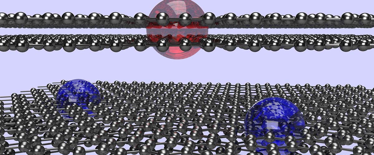
TALLAHASSEE, Fla. — Ultra-thin materials have been taking the research world by storm for more than a decade, with scientists optimistic that they will lead to new and exciting electronic and quantum technologies. However, these single atomic layers of materials need to be “stitched” together to unlock their full potential, a particularly complex process when it comes to certain semiconductors known as transition-metal dichalcogenides. And some specialized applications, including so-called complementary logic electronics, require stitching these compounds over a large area.
Researchers from the University of South Florida (USF) have developed a groundbreaking method to join these atomically thin semiconductors. This new approach yields high-quality structures that scientists can use to develop prototype devices such as junctions, which form the basis of diodes and photovoltaic cells.
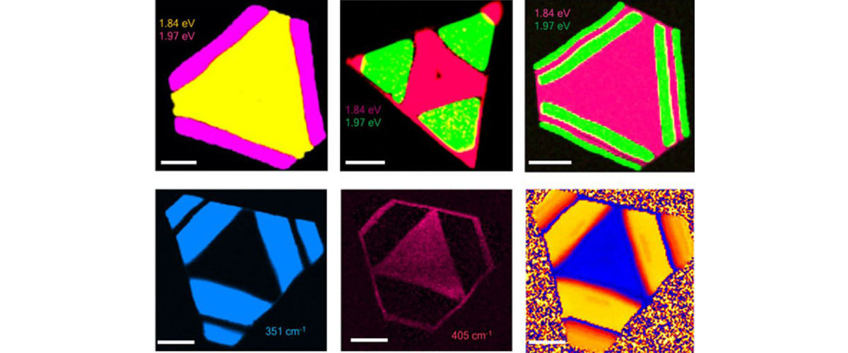
The structural uniformity and the electronic properties of these structures were characterized by researchers at the National High Magnetic Field Laboratory. Their work was published in Nature on January 3.
“This method allows us to perform multiple chemical reactions within one single reaction chamber,” explains MagLab physicist Luis Balicas. “By regulating the exact gas composition within the reaction chamber, our colleagues at USF realized that one could control the growth of each material independently and create many different junctions continuously.”
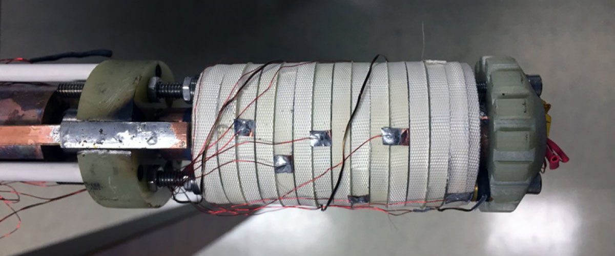
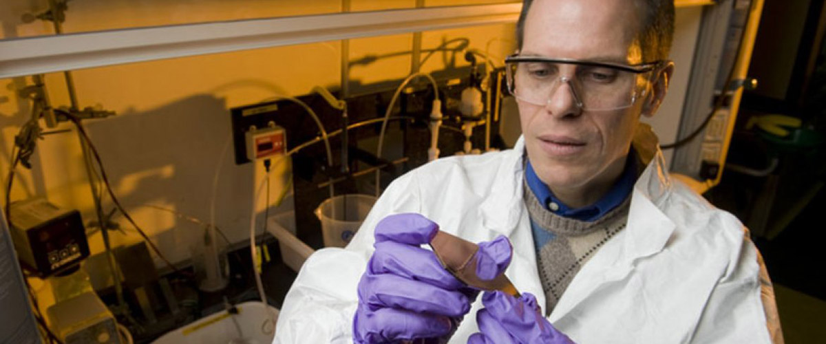
Researchers used the National MagLab’s high-resolution aberration corrected electron microscope to observe the interface quality between semiconductors at the atomic scale. Combining that information with electronic measurements made at the MagLab, researchers confirmed that this stitching method is both flexible and scalable, with potential to make even larger impacts ahead in niche applications that may require transparency, flexibility and low weight.
“This process is relatively simple, low cost and extendable to a number of other two-dimensional materials,” Balicas explains. “It lays the foundation for the fabrication of complex planar superstructures which are the building blocks of electronic devices and integrated circuits.”
Story by Kristin Roberts