The MagLab is funded by the National Science Foundation and the State of Florida.
The MagLab is funded by the National Science Foundation and the State of Florida.
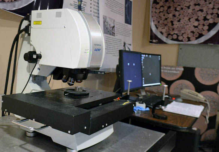
The Applied Superconductivity Center is home to many unique instruments, facilities, and capabilities. Explore them in more detail here.
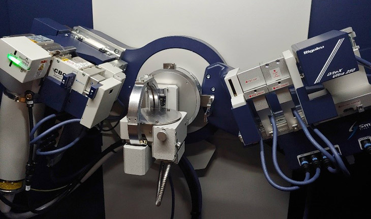
Rigaku SmartLab SE X-Ray Diffractometer (Shaw 148)
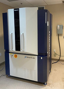
Description: This X-ray diffraction system features a 3 kW x-ray generator that is fully integrated within an automated X-ray diffraction system. The system uses a 2.2 kW Cu X-ray tube with an electromagnetic shutter and has Cross Beam Optics (CBO) with a Parabolic Mirror, and user selectable Parallel Beam and Bragg-Brentano optical configurations for asymmetric and symmetric scanning geometries. The Ge (220) 2-bounce high-resolution channel-cut incident beam monochromator gives us high-resolution parallel beam measurements of the crystal structure of imperfect materials. It has a high accuracy vertical theta-theta goniometer system with open architecture design for horizontal sample mounting and measurement. The motorized horizontal stage means that samples do not need to be clamped. The detector is an extremely fast D/teX Ultra 250 High Speed 1D Silicon Strip Detector.
Specifications:
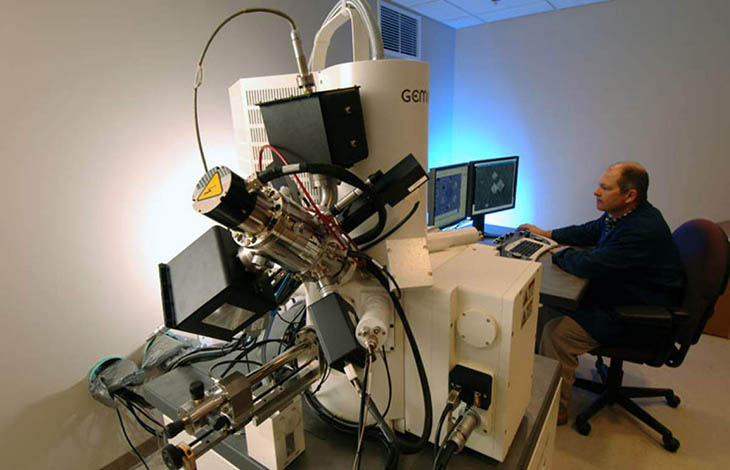
Bob Goddard uses the Zeiss 1540 EsB crossbeam scanning electron microscope
This multifunctional tool has many advanced features:
This system is ideally suited to providing electron-transparent sample for imaging in the MagLab’s spherical aberration probe corrected JEM-ARM200cF sub-Å resolution scanning transmission analytical electron microscope.
Information on how this instrument is being used is available on our scheduling page (accessible only to MagLab and FSU staff) and by contacting Yan Xin.
Credit: National MagLab

Low temperature laser scanning microscope.
This technique allows us to visualize the voltage change responses on local heating from low power diode laser at constant bias current at temperatures 3.7 K – 300 K with magnetic fields up to 5 tesla.
In experiments with thin film superconductors the voltage change response is proportional to the local electric field, while a sample is cooled below the transition temperature and biased with current above the critical current. The laser microscope is capable of measuring simultaneously the voltage change response with resolution down to 2-3 μm and the intensity of reflected light with resolution <1 μm.
Magneto-optic imaging facility
Magneto-optical imaging allows us to image and measure the local uniformity of current flow or magnetization in fields up to 0.15 T and temperatures down to ~6 K using the Faraday effect by applying an in-plane magnetized Bi-YIG imaging film to the sample surface and imaging using polarized light microscopy.
Facilities include:
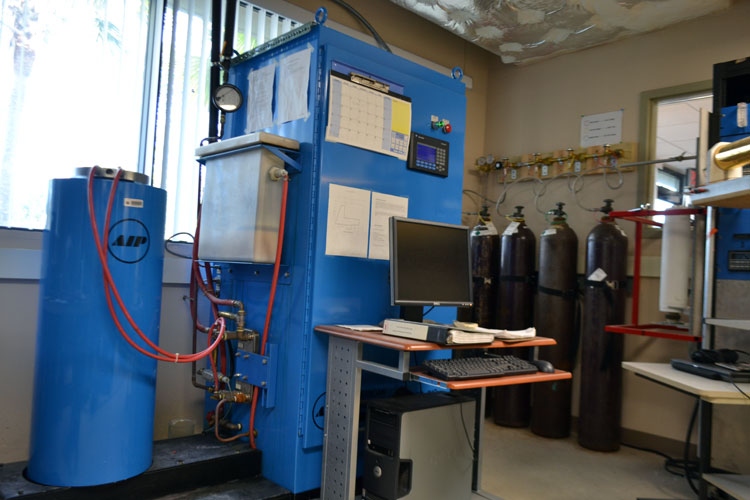
A wide range of furnaces are available for heat treating in air, vacuum and special atmospheres, for example pure O2.
Credit: National MagLab
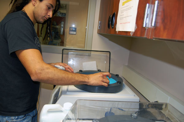
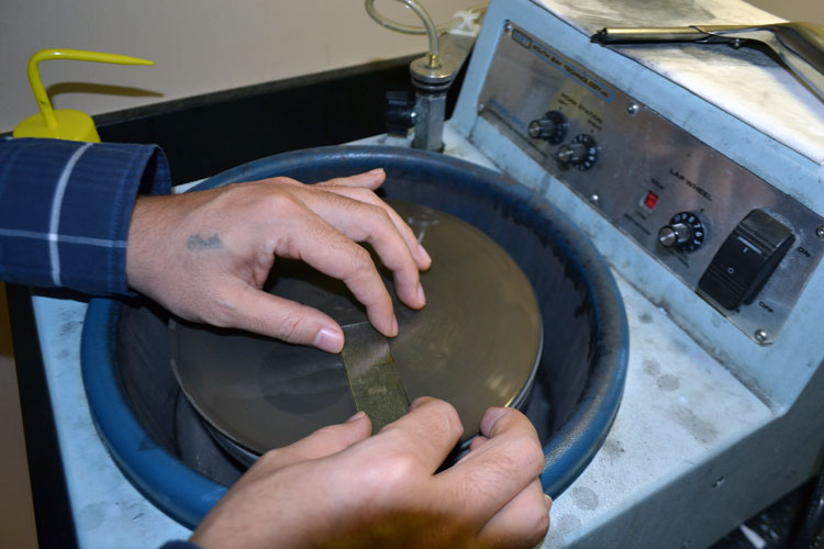
An extensive metallographic preparation laboratory allows preparation of complex structures with minimal polishing artifacts from initial diamond saw sectioning to final vibratory polishing.
Credit: National MagLab

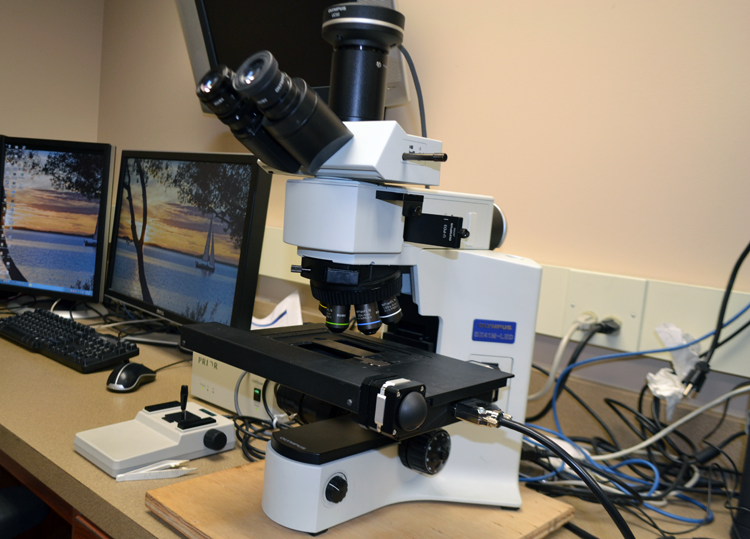
Scanning laser confocal microscope
The scanning laser confocal microscope (SLCM, Olympus OLS 3100) is a high resolution light microscope with a 10 nm depth resolution and 0.12 µm spatial resolution.
It provides us with non-contact topographic measurements that can be used to make volumetric and surface roughness measurements. The digitally controlled stage allows us to automatically collect very high pixel count mosaics so that large areas can be covered at high resolution.
Information on how this instrument is being used is available on our scheduling page (accessible only to MagLab and FSU staff) and by contacting Peter Lee.
This lab provides high precision tripod polishing for TEM samples and BCP and EP polishing for SRF samples.
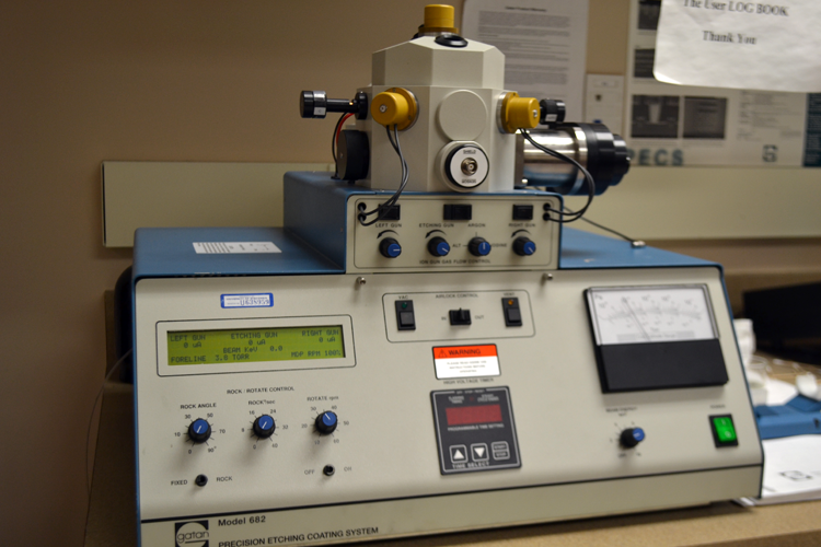
This supplements the main MagLab TEM sample preparation laboratory that includes a Gatan dimpler, Gatan Precision Ion Polishing System (PIPS), Gatan Solarus™ (Model 950) Advanced Plasma Cleaning System and a Fischione ion mill.
Credit: National MagLab

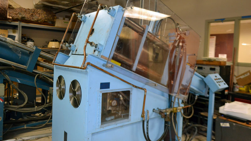
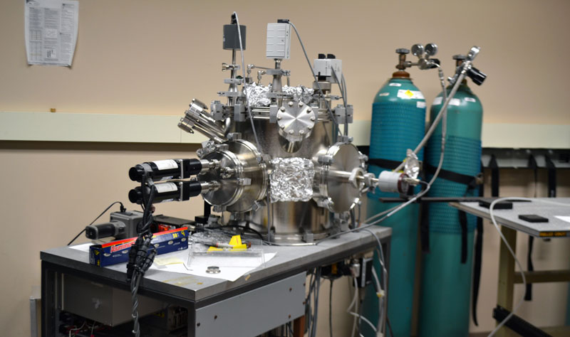
Complex and high quality single and multilayer structures can be grown using our Pulsed Laser Deposition Facility (Lambda Physik LPX® 210i, KrF excimer laser) with dielectric rare mirror for 248 nm with a Neocera deposition chamber and 6-target.
Credit: National MagLab


Last modified on 18 December 2025