Nb-47wt.%Ti alloy has become the dominant commercial superconductor because it can be economically manufactured in a ductile form with the prerequisite nano-structure needed for high critical current density generated by strong vortex pinning. Similarly Nb3Sn, although based on a brittle A15 intermetallic phase, can be manufactured into strong composites in km lengths with fine-grain nanostructures with high critical current densities. Nb-Ti and Nb3Sn are often termed "technical superconductors" because more than 95% of all superconducting magnets have been made with them. They typically require cooling to 4.2 K (liquid He is the most common coolant) and in some instances to below 2 K (superfluid liquid He) as in the case of the Large Hadron Collider (LHC) and typical Nb-based Superconducting Radio Frequency Cavity (SRF) applications. Occasional use at higher temperatures up to about 6 K in He gas occurs too.
CERN Nb-Ti Reference Strand for the LHC Project containing over 6000 Nb-47Ti filaments
Work in the Applied Superconductivity Center (ASC) has since the late 1970’s centered on understanding and improving these conductors for High Energy Physics and Fusion applications, but our advances have benefited the full range of LTS superconductor applications, including MRI and NMR devices.
A key feature of the work at ASC has been the integration of processing, the microstructure developed by fabrication and detailed superconducting property characterization. ASC has an extensive facility for superconducting property measurements which are combined with the center's own metallographic laboratory and the state-of-the-art instruments at the Magnet Lab. In addition the center has a unique industrial quality wire fabrication facility that includes a hydrostatic extrusion press. The result has been a continuous output of landmark papers underpinning the huge improvement of LTS properties in the last 30 years
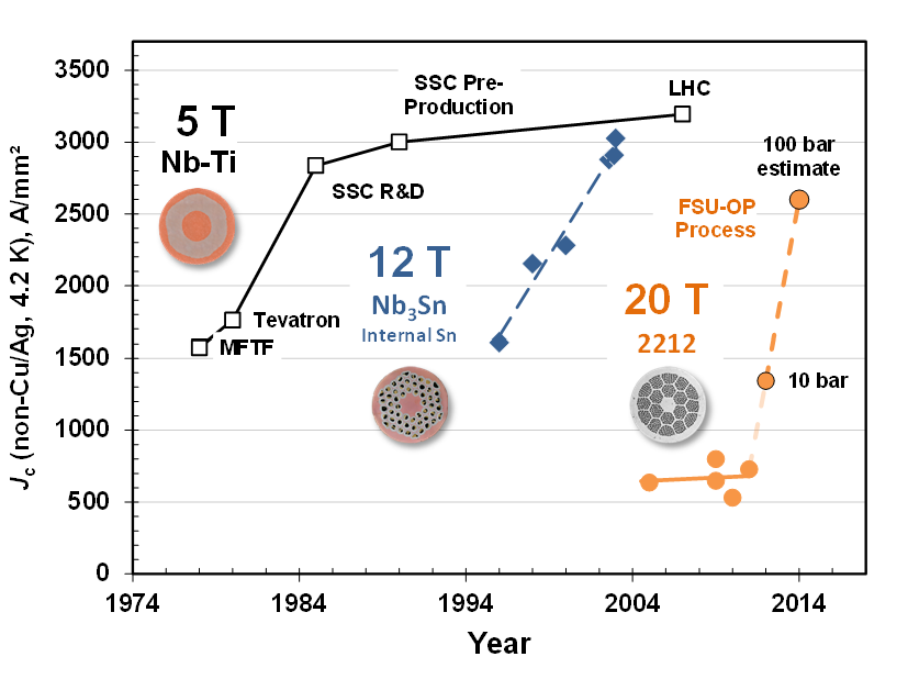
Progress in Nb-Ti, Nb3Sn and Bi-2212 (coil-tested JE(4.2 K) values only). Note that all three conductors are round, multifilament, twisted and stabilized with high purity normal metal.
Research Focus
The core for our current work (2014) is the development and understanding of Nb3Sn for applications in the 12-16 T field range and of Nb for superconducting radio frequency (SRF) cavity application. We center this effort on:
Understanding what controls the A15 composition and microstructure and how this controls flux pinning
Being produced by a diffusion process that does not proceed to equilibrium, Nb3Sn wires have a range of composition (˜18-25 at.%Sn) and a range of Tc (˜6-18 K). They are longitudinally uniform but radially non-uniform. Understanding real and complex wires requires knowledge of the micro-chemistry, the micro-structure and the local superconducting properties, often at the nano-scale since the superconducting coherence length ζ is only 3 nm. We have developed new techniques to monitor compositional changes at this scale using measurements of the specific heat, which can be correlated to analytical scanning and transmission electron microscopy (TEM, STEM and SEM) at many scales from the picometer to the centimeter scales. Key issues are control of grain size below ˜100 nm, minimization of composition gradients in the Nb3Sn phase, prevention of filament intergrowths and prevention of tin diffusion barrier breakdown. Our global goal is to drive the critical current density (Jc) of the A15 layer as high as it can go. A present goal is to understand the specific grain boundary pinning force, QGB, and to understand whether nanometer segregations of Cu and Ti to the GB benefit or harm QGB.
Understanding the magnetic field temperature phase diagram
Superconductivity occurs only within a phase field defined by the upper critical field Hc2 and the transition temperature, Tc. Both Hc2 and Tc vary strongly with composition of the A15 phase (which is determined by the reaction conditions), the prestrain, and by alloying with Ti, Ta or other elements that can enhance the conductor properties. Recent work of our graduate students on internal-Sn and Powder-in-Tube (PIT) composites has made it clear that several present high-Jc internal Sn composites are failing to optimize their primary properties (Tc and Hc2). It seems likely that this is contributing to significant loss of Jc (12 T) in conductors. These results help explain the remarkable recent progress in HEP Nb3Sn strand, that now exceeds the previous design goal of 3000 A/mm² (12 T, 4.2 K). We seek to exploit this understanding by working with industry (see below) to further improve the properties of the strand.
Detailed studies of high Jc internal Sn and powder-in-tube (PIT) conductors
Our studies of high-Jc PIT and internal-Sn conductors have shown that both conductors have a Jc, Tc and Hc2 performance that is remarkably sensitive to composition and compositional uniformity.
Monitor and support industrial developments
There have been remarkable developments from industry in recent years and this has been bolstered by the US-DOE HEP Conductor Development Program. We support these developments by using our unique range of facilities to provide measurements of Tc, H*, Hc2, grain size, component ratios and Qgb, in collaborations with Brookhaven National Laboratory, Berkeley Lab, CERN and NIST.
Model A15 composite fabrication
Our integrated facilities for superconductor fabrication and characterization are among the most advanced and comprehensive of any university facility. We are using our HIP'ing and extrusion facilities to produce micro-chemically homogeneous A15 in order to study directly the effects of composition on primary superconducting properties.
Nb3Sn strand and conductor for ITER
The magnetic confinement fusion reactor, ITER, being constructed in Cadarache, France, is the largest application of Nb3Sn yet; 380 tons for the Toroidal Field (TF) magnets and 122 tons for the Central Solenoid (CS) magnets. The high magnetic fields produced by the magnet systems generate Lorentz forces on the strands that can alter their properties over the lifetime of the machine. In a collaboration with ITER, the University of Twente, and CRPP we have been studying the strand and conductor properties for both the CS and TF systems so that the design and lifetime can be improved.
Nb for SRF
We are using our unique combination of micro-analytical tools and expertise to investigate the surface superconducting properties of high purity Nb in collaboration with Michigan State University, Fermilab and Jefferson Lab.
Recent Publications
Examination of the trade-off between intrinsic and extrinsic properties in the optimization of a modern internal tin Nb₃Sn conductor, Superconductor Science and Technology 27 065013. Read online …
In modern Nb3Sn wires there is a fundamental compromise to be made between optimizing the intrinsic properties associated with the superfluid density in the A15 phase (e.g. Tc, Hc, Hc2, all of which are composition dependent), maximizing the quantity of A15 that can be formed from a given mixture of Nb, Sn and Cu, minimizing the A15 composition gradients within each sub-element, while at the same time generating a high vortex pinning critical current density, Jc, by maximizing the grain boundary density with the additional constraint of maintaining the RRR of the Cu stabilizer above 100. Here we study these factors in a Ta-alloyed Restacked-Rod-Process (RRP®) wire with ˜70 μm diameter sub-elements. Consistent with many earlier studies, maximum non-Cu Jc(12 T, 4.2 K) requires preventing A15 grain growth, rather than by optimizing the superfluid density. In wires optimized for 12 T, 4.2 K performance, about 60% of the non-Cu cross-section is A15, 35% residual Cu and Sn core, and only 5% a residual Nb7.5wt.%Ta diffusion barrier. The specific heat and chemical analyses show that in this 60% A15 fraction there is a wide range of Tc and chemical composition that does diminish for higher heat treatment temperatures, which, however, are impractical because of the strong RRR degradation that occurs when only about 2% of the A15 reaction front breaches the diffusion barrier. As this kind of Nb3Sn conductor design is being developed for sub-elements about half the present size, it is clear that better barriers are essential to allowing higher temperature reactions with better intrinsic A15 properties. In this paper we present multiple and detailed intrinsic and extrinsic evaluations because we believe that only such broad and quantitative descriptions are capable of accurately tracking the limitations of individual conductor designs where optimization will always be a compromise between inherently conflicting goals.
Sung Z-H, Lee P J and Larbalestier D C 2014 Observation of the Microstructure of Grain Boundary Oxides in Superconducting RF-Quality Niobium With High-Resolution TEM (Transmission Electron Microscope), IEEE Transactions on Applied Superconductivity 24 68–73. Read online …
All superconducting RF (radio-frequency) cavities are currently manufactured using high purity Nb sheet and although properties of the best cavities are excellent there is still considerable variability and we examine here the chemistry at the Nb grain boundaries, which may be a source of cavity performance degradation. Some oxidization at grain boundaries (GBs) in niobium cavities may be inevitable during the long cavity fabrication process; due to the formation of hydrosoluable niobium oxide phases during the surface removal procedure, grain boundaries in SRF Nb can be easily attacked, resulting in the formation of uncontrolled complex niobium oxides at the grain boundaries. These GB oxide phases can significantly suppress local surface superconductivity during RF cavity operation. Thus observation of the GB oxide structure with high resolution TEM (transmission electron microscope) has been attempted to identify the microstructural details that affect SRF Nb cavity performance. In this study, we developed a TEM sample preparation technique for producing damage-free SRF NB samples with good electron-transparency using metallographic and FIB (focused ion beam) methods. These sample preparation techniques enabled us to successfully observe the microstructure of a variety of grain boundaries with high resolution TEM. TEM BF (bright field) images showed that optimized cavity surface treatment can generate impurity segregations, oxide phases, and dislocation-pile-ups at the vicinity of the grain boundaries in SRF Nb. These surface defects are predicted to be strong sources for localized degradation of surface superconductivity and these results help explain previous magneto optical (MO) measurements that showed early magnetic flux penetration along the grain boundary of BCP’ed Nb bi-crystal under DC condition.